When designers design analog electronics they often divide the design in smaller sub systems. When this is done correctly it allows designers to specify parameters of the different sub systems such that when they are combined the resulting circuit meets all specified requirements.
In electronics textbooks the classification of the different subsystems is often not explicitly described. For this post the elementary signal processing functions off [1] will be used. This classification makes use of 5 classes of signal processing functions: generation, dissipation, transformation, replication and combination [1].
The resistor divider can be categorized in two of the aforementioned classes, generation and transformation. The actual categorization would depend on why the resistor divider is being used. When the resistor divider is used as a reference it would fall under the generation class while if it is used as an attenuater it would fall under the transformation class.
To determine if a resistor divider could be used in a design its properties should be known. Because it is a simple circuit it might not always suffice however it is important to know when a more complex circuit is or isn’t needed.
Signal transfer
The transfer function of a resistor divider as shown in figure 1 is given by equation 1. There are multiple circuit analysis methods of deriving equation 1 from the schematic shown in figure 1.
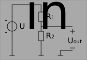
One method is to calculate the total current flowing through R_1 and R_2 and multiplying this current with R_2. This wil result in an equation that calculates the output voltage based on the input voltage, after dividing both sides of the equation over the input voltage the transfer function of equation 1 is found.
H=\frac{R_2}{R_1+R_2} \tag{1}
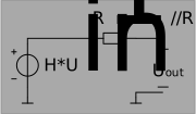
If the resistor divider is used to create a reference voltage it can be useful to determine the equivalent Thévenin circuit. This equivalent circuit is shown in figure 2. An often undesired effect of the resistor divider is its high output impedance created by the Thévenin resistor. However sometimes this output impedance can be used as an advantage by choosing R_1 and R_2 such that the Thévenin resistance becomes one that is needed in the design.
Since in most cases the output impedance of the resistor divider is unwanted it can be minimized through the addition of a capacitor. This capacitor should be placed at the output of the resistor divider since it then creates a low pass filter, as shown in figure 3. The capacitor adds a pole to the
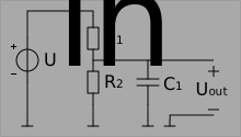
From figure 3 a new transfer function can be calculated. This new transfer function is shown in equation 2. From equation 2 it can be seen that it has a frequency dependant behavior. This is because C_1 adds a pole to the transfer function. The location of this pole is given by equation 3. Note the pole location calculated with equation 3 is in radians per second!
H\left(\omega\right)=\frac{R_2}{R_1+R_2}\frac{1}{1+j\omega\frac{R_1R_2}{R_1+R_2}C} \tag{2} p=-\frac{1}{\frac{R_1R_2}{R_1+R_2}C} \tag{3}
The pole from equation 2 can also be found using the Thévenin equivalent circuit of the resistor divider. With the Thévenin equivalent circuit a low pass RC circuit as shown in figure 4 is found. Where the resistor of the RC low pass filter is given by the Thevenin equivalent resistance of the resistor divider.
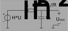
The add capacitor (C_1) causes the output impedance of the reference implemented with a voltage divider to decrease. From figure 4 it can be concluded that for the goal of limiting the output impedance of the resistor divider the capacitor C_1 can be placed in parallel with either R_1 or R_2. There is however a good reason to not place the capacitor C_1 in parallel with R_1, this reason will be shown in the next section.
Power supply rejection ratio
If the resistor divider is used to implement a voltage reference AC changes on the power supply should not change the reference output voltage. A figure that describes how well a reference rejects changes of its power supply to its output is the power supply rejection ratio (PSRR) [2]. The PSRR is calculated with equation 4.
PSRR=\frac{U_{sup}}{U_{out}} \tag{4}
For the resistor divider without a capacitor (see the schematic in figure 1) the PSRR is constant over frequency and given by equation 5 [2]. From equation 5 it can be seen that if a high PSRR is wanted R_1 must be much larger then R_2.
PSRR=1+\frac{R_1}{R_2} \tag{5}
When the output of the reference has been determined (for example 2V5) and a high PSRR is required (for example PSRR>100) then a very high power supply voltage may be needed (in case of the example 250 volt). If the PSRR mostly matters for frequencies higher then 0 Hz the previously placed capacitor from figure 3 can be used.
PSRR\left(\omega\right)=1+\frac{R_1}{R_2}+j\omega R_1C_1 \tag{6}
Since C_1 in figure 3 created a low pass filter as shown in figure 4 C_1 will attenuate all signals past the cut off frequency formed by R_1//R_2 and C_1. If C_1 would have been placed in parallel with R_1 in figure 3 then the Thévenin schematic changes from figure 4 to that of figure 5. From figure 5 it can be seen that for increasing frequencies the PSRR would go to 1, which is undesirable.
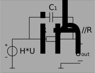
The point from which the PSRR will increase is given by the location of the null in equation 6, this null is given by equation 7. Interesting to note is that the null of the PSRR is located at the same frequency as the pole of the output impedance. This is because when the resistor divider is used as a voltage reference its PSRR function is the inverse of its transfer function.
n=-\frac{1}{\frac{R_1R_2}{R_1+R_2}C} \tag{7}
Power consumption
In cases where a voltage reference is used in a low power application its implementation may not draw to much power. If a resistor divider were to be used its power consumption should be determined. In the case of the resistor divider its quiescent power draw can be calculated with equation 8.
P=\frac{U_{sup}^2}{R_1+R_2} \tag{8}
Conclusion
If a electronics designer, student, hobbyist or someone else wants to implement a voltage reference or attenuator they can use the equations shown in this post to determine if a resistor divider can be a viable implementation. It is possible that if enough requirements have been set specific component values can be calculated or at least ratios of components to meet a set of specifications.
This is not the final version of this post. In the future it will be edited to add a section about the voltage noise generated by the resistors and how that effects the output in case of a voltage reference or the input in case of an attenuator. Also there will be a section added about tolerances of the components, and if time permits a section will be added with one or more design examples.